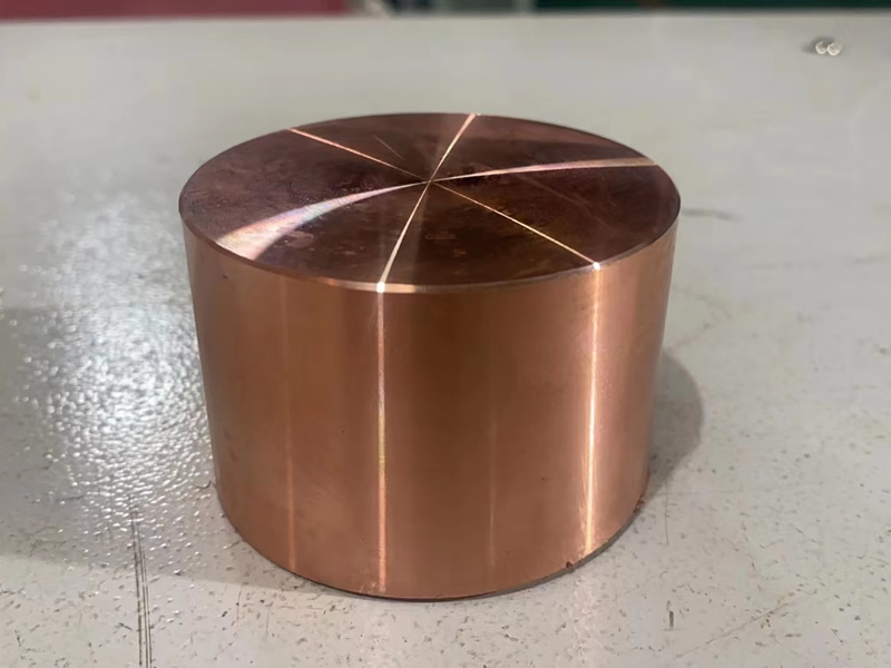
Global Copper Sputtering Target Market Definition
Physical vapor deposition (PVD), a method that involves the high-velocity ejection of atoms from solids, is applied to materials that are used as sputtering targets. After depositing on the workpiece, the atoms are expelled, creating a thin film coating that has advantageous qualities. When high-energy ions collide with the atoms of the target substance, momentum is transferred. Occasionally, many collisions can happen. The ions occasionally experience energy loss during long-distance flight. The atoms colliding will separate from the target material, a process known as sputtering, if the energy of the ions traveling to the target is larger than the energy of the bonds holding the target material’s atoms together. And during copper sputtering, a kind of deposition method, thin coatings on the target with a thickness ranging from a few nanometers to a few micrometers are produced.
Targets for sputtering are frequently used to cover electronic equipment and parts. Copper is increasingly used in large-format, high-resolution TFT-LCD television screens due to its excellent electrical conductivity. The electrode layer of thin-film transistors is made of copper. The quality of the resulting image is determined by the copper layer, which regulates the individual image dots (or pixels). You gain homogeneous erosion and low sensitivity to particle formation throughout the sputtering process thanks to the exceptionally fine-grained microstructure of our copper sputtering targets. In the vacuum coating industry, the copper sputtering target is a great sputtering material. Sputtering targets are a unique class of materials, particularly for thin film coating, and the copper sputter target is the end result of several procedures on high-purity copper metal. It is a certain size and shape.